FPGA design
This chapter describes the FPGA design that will be used on the target platform. It will utilize Zynq US+ MPSoC’s PCIe hard block and additional supporting logic to handle NVMe physical layer and expose the NVMe configuration registers and DMAs to the RPU.
A diagram that presents the connections between various elements of the design is shown below:
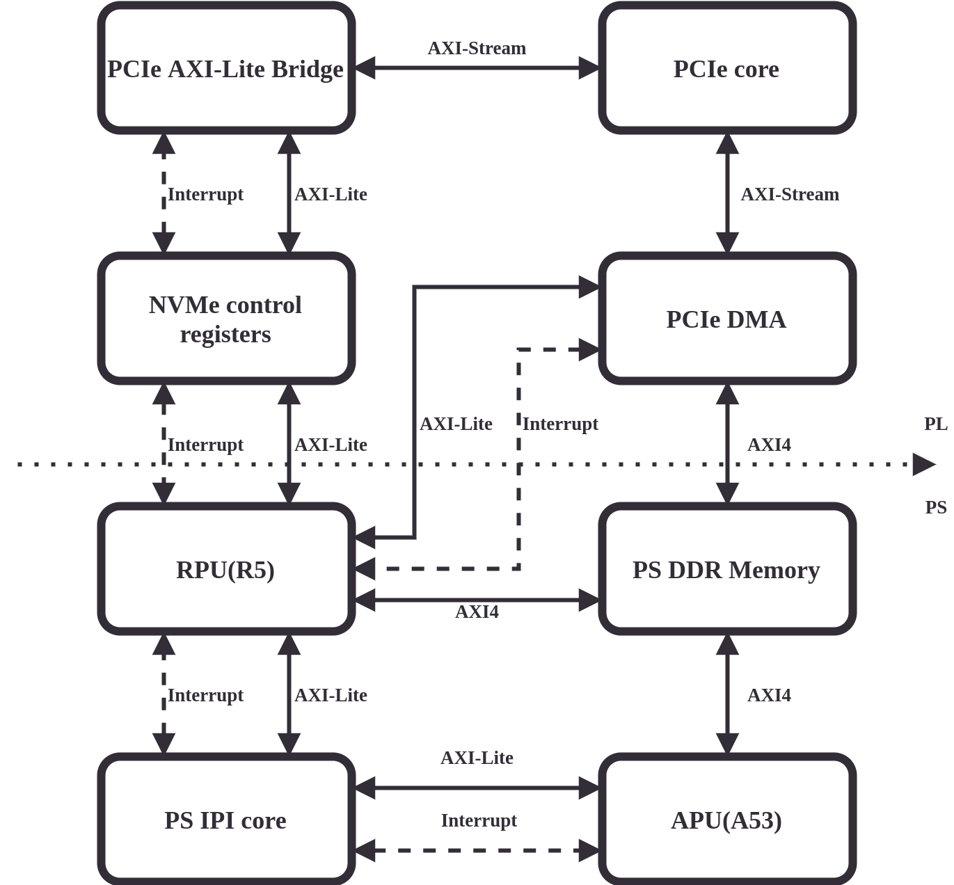
There are four major parts that can be distinguished:
PCIe core, which will handle the basic PCIe protocol and will provide:
Host access to NVMe control registers using BAR space
Access to Host memory for PCIe DMA.
Support for generating Host interrupts.
The RPU core, NVMe control reigsters and PCIe DMA that will be responsible for handling the base NVMe protocol:
RPU will implement NVMe handling logic.
NVMe control registers will provide register space required by the NVMe specification and will generate required interrupts, e.g. on writes to
Doorbellregisters).PCIe DMA will be responsible for transferring data to and from the Host memory.
The APU core and PS IPI core that will be responsible for handling custom NVMe commands:
The IPI core will be used to communicate between RPU and APU.
APU will implement logic that handles custom NVMe commands.
Shared PS DDR memory will be used by both APU and RPU cores and will be used as buffer before transferring NVMe data to/from the Host.
Building the design
Instructions for building the design (and the whole project) are present in the alkali-csd-projects README and alkali-csd-hw README.
Note
Building the design will require Vivado 2019.2 to be installed on the development PC.
NVMe register module
The NVMe register module is an IP core written in Chisel that implements Controller Registers described in the NVMe Specification.
The register map follows the register layout from the specification and by default contains 5 pairs of doorbell registers.
On top of implementing basic Controller Registers, this module contains additional logic that is used by the firmware running on the RPU for:
Generating RPU interrupts on Host writes
On each Host write, register address is saved to Host Write Address FIFO which can later be accessed by the RPU to see which registers have been written and require action.
Generating Host interrupts
RPU can trigger one of the 32 MSI interrupts by writing to a control register with correct bits set, e.g. writing a value with bit 31 set sends interrupt 31.
To be able to use those additional features, the core contains three additional registers:
Interrupt Status Register - by default located at
0x1028which returns1when there is at least one entry in Host Write Address FIFO.Interrupt Data Register - located at
0x102creturns oldest entry from Host Write Address FIFO when read.Host Interrupt Register - located at
0x1030triggers Host interrupt when written.
Generating NVMe IP
NVMe IP is written in Chisel which means that synthesizable Verilog must be first generated from sources. The sources for generating NVMe IP is present in alkali-csd-hw/tree/main/chisel.
It is built within alkali-csd-hw build flow, described in its README.
To just generate the NVMe IP, the following dependencies are required:
Scala (2.13.0)
SBT
Java
Note
A Dockerfile for building HW artifacts is a recommended environment for generating the NVMe IP.
Once the dependencies are present, run:
git clone https://github.com/antmicro/alkali-csd-hw.git
cd chisel
make verilog
Updating register definitions
You can update the register definitions using nvme-registers-generator.
Those generator scripts take the NVMe Specification .pdf file as an input and based on that generate register definitions that can be used in Chisel.
For details on generating register definitions check the nvme-registers-generator README file in the repository.
Adding new registers
NVMe IP can be expanded with additional registers, either unimplemented optional ones or vendor specific.
To add a new register, you can use the following steps:
Check if your register layout is defined in
RegisterDefs.scala(this only applies if you want do add an unimplemented register). Take a look intoCSRRegMap.scalaif your register was already defined - it might be already present as a simpleStorageRegister.Add new register layout definition to
CSR.scalaif needed.IRQHOSTcan be used as an example:class IRQHOST extends RegisterDef { val REQ = UInt(32.W) }
Instantiate new register as a module in
CSRFile.scala, make all needed connections and add it toregMap.IRQHOSTcan be used as an example:val irqHost = Module(new AutoClearingRegister(new IRQHOST, dataWidth)) println(f"adding Host interrupt register at 0x${irqHostBase}%x") regMap(irqHostBase) = irqHost io.irqHost := irqHost.fields.REQ
VTA module
The VTA is an IP core written in HLS that is used by TFLite to accelerate certain operations. You can find more information about using it in VTA accelerator.
To build the VTA and whole HW design, follow the README in alkali-csd-hw.
Built artifacts
The ready-to-use binaries for the hardware are available under alkali-csd-hw releases.