DDR5 Test Board
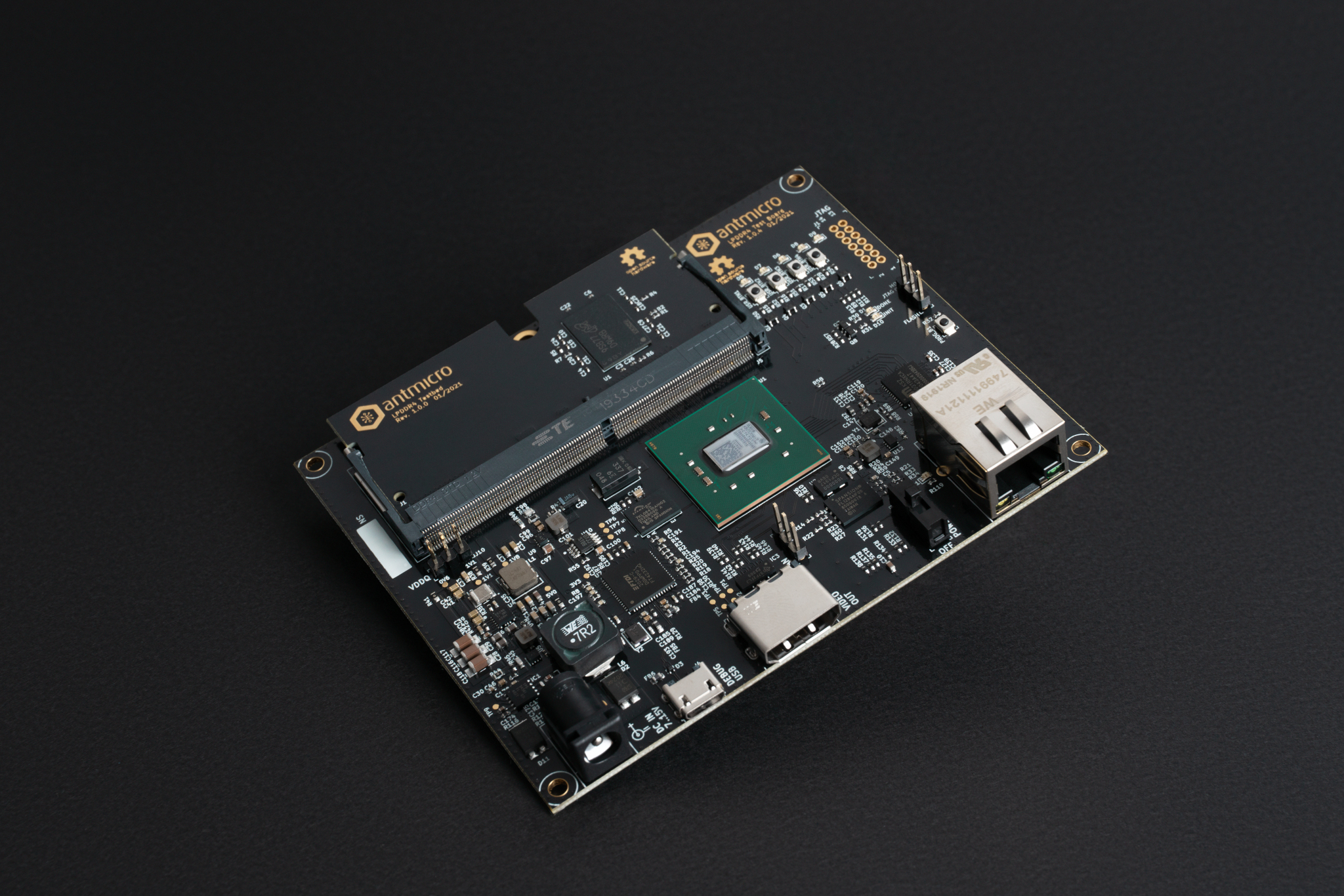
The DDR5 test board is an open source hardware test platform that enables testing and experimenting with various x4/x8 DDR5 modules embedded on DDR5 testbed.
The hardware is open and can be found on GitHub:
The following instructions explain how to set up the board.
Board configuration
First connect the board USB and Ethernet cables to your computer, plug the board to the socket and turn it on using power switch. Then configure the network. The board’s IP address will be 192.168.100.50 (so you could e.g. use 192.168.100.2/24). The IP_ADDRESS environment variable can be used to modify the board’s address.
Next, generate the FPGA bitstream:
export TARGET=ddr5_test_board
make build TARGET_ARGS="--l2-size 256 --build --iodelay-clk-freq 400e6 --bios-lto --rw-bios --no-sdram-hw-test"
Note
–l2-size 256 sets L2 cache size to 256 bytes
–no-sdram-hw-test disables hw accelerated memory test
Note
By typing make (without build) LiteX will generate build files without invoking Vivado.
The results will be located in: build/ddr5_test_board/gateware/antmicro_ddr5_test_board.bit. To upload it, use:
export TARGET=ddr5_test_board
make upload
To save bitstream in flash memory, use:
export TARGET=ddr5_test_board
make flash
Warning
There is a JTAG/SPI jumper named MODE2 on the right side of the board.
Unless it’s set to the SPI setting, the FPGA will load the bitstream received via JTAG.
Bitstream will be loaded from flash memory upon device power-on or after a PROG button press.