LPDDR4 Test Board
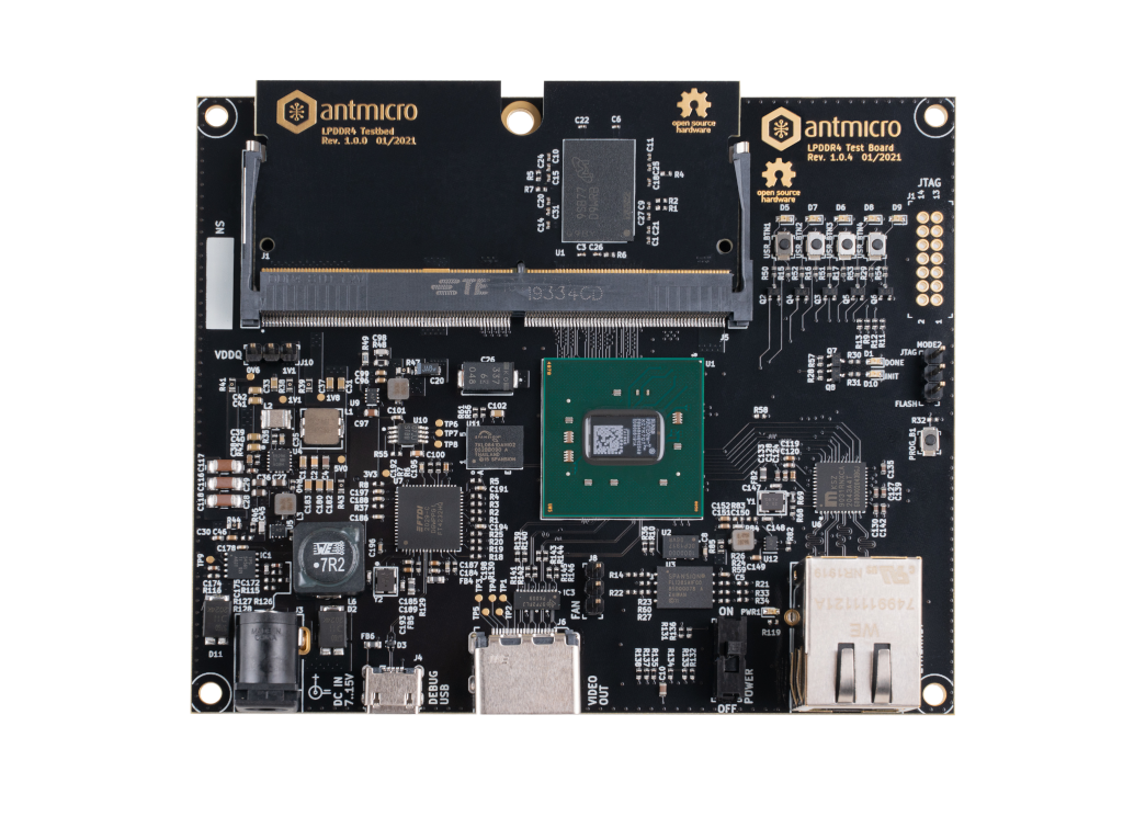
Fig. 10 LPDDR4 Test Board
The LPDDR4 Test Board is a platform developed by Antmicro for testing LPDDR4 memory. It uses the Xilinx Kintex-7 FPGA (XC7K70T-FBG484).
The hardware is open and can be found on GitHub (https://github.com/antmicro/lpddr4-test-board).
This Test Board supports interchangeable Test Beds that can be populated with various memories. Initially the LPDDR4 Test Board was meant to be used with LPDDR4 Test Beds. Currently it also supports DDR5 Test Beds.
For FPGA digital design documentation for this board, refer to the Digital design chapter.
IO map
A map of on-board connectors, status LEDs, control buttons and I/O interfaces is provided in Fig. 11 below.
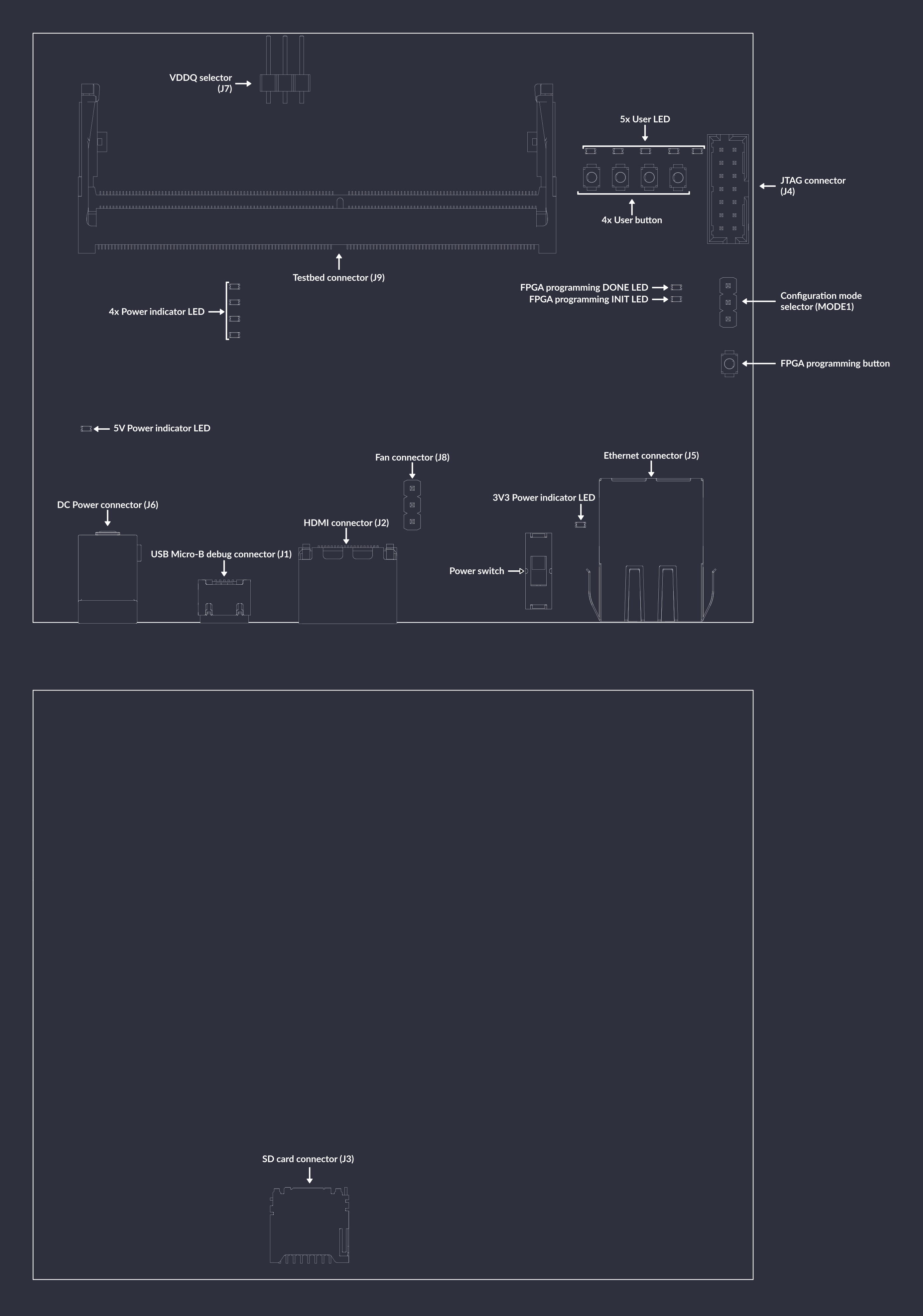
Fig. 11 LPDDR4 test board interface map
Connectors:
J6- main DC barrel jack power connector, voltage between 7-15V is supportedJ1- USB Micro-B debug connector used for programming FPGA or Flash memoryJ4- standard 14-pin JTAG connector used for programming FPGA or Flash memoryJ2- HDMI connectorJ5- Ethernet connector used for data exchange with on-board FPGAJ9- 260-pin SO-DIMM connector for connecting LPDDR4 memoryMODE1- configuration mode selector, short proper pins with jumper to specify programming modeJ7- VDDQ selector used for specifying value of VDDQ voltageJ8- optional 5V fan connectorJ3- socket for SD card
Switches and buttons:
Power switch
S1- slide up to power up a device, slide down to turn the device offFPGA programming button
PROG_B1- push to start programming from Flash4x User button (
USR_BTN1,USR_BTN2,USR_BTN3,USR_BTN4) - user-configurable buttons
LEDs:
Power indicators (
PWR1,PWR2,PWR3,PWR4,PWR5,PWR6) - indicates presence of stabilized voltages: 5V, 3V3, 1V8, 1V2, 1V1, 1V0FPGA programming INIT
D9- indicates current FPGA configuration stateFPGA programming DONE
D8- indicates completion of FPGA programming
Board configuration
First insert the LPDDR4 testbed into the socket J9 and make sure that jumpers are set in correct positions:
the VDDQ switch (
J7) should be set in the1V1positionMODE1switch should be set in the FLASH position
Connect power supply (7-15VDC) to J6 barrel jack.
Then connect the board’s USB-C J1 and Ethernet J5 interfaces to your computer.
Turn on the board using power switch S1.
Then configure the network.
There is a JTAG/FLASH jumper MODE1 on the right-hand side of the board.
It defines whether the bitstream is loaded via JTAG or FLASH memory.
The bitstream will be loaded from flash memory upon device power-on or after the FPGA programming PROG_B1 button is pressed.