RDIMM DDR4 Tester

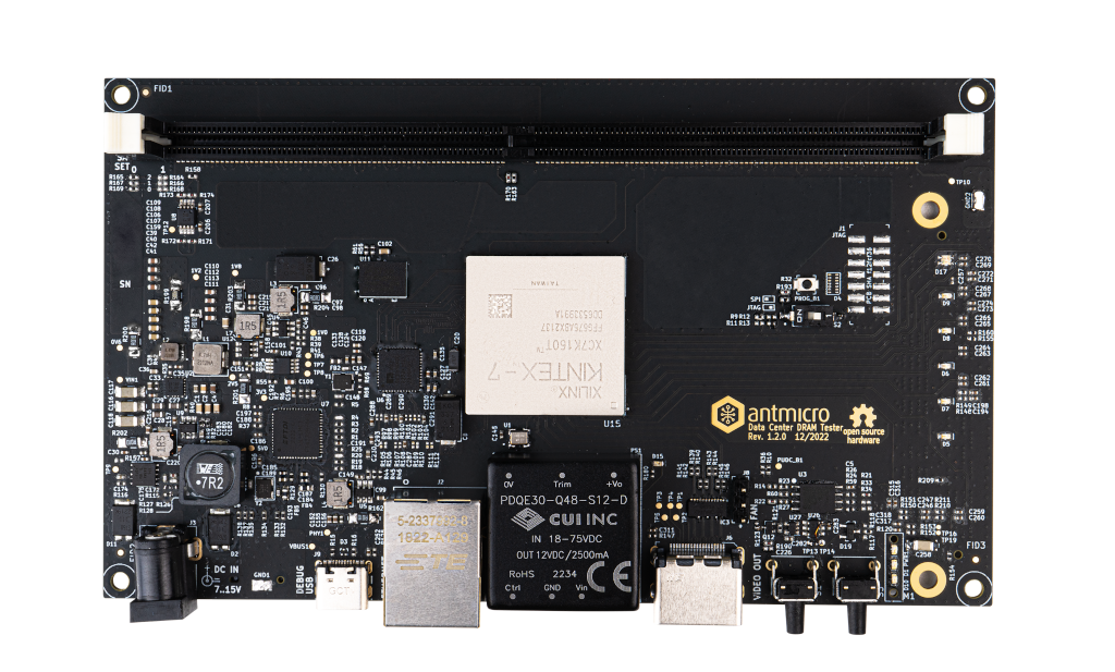
Fig. 8 Data Center RDIMM DDR4 Tester
The Data Center RDIMM DDR4 Tester is an open source hardware test platform that enables testing and experimenting with various DDR4 RDIMMs (Registered Dual In-Line Memory Module).
The hardware is open and can be found on GitHub: https://github.com/antmicro/rdimm-ddr4-tester
The following instructions explain how to set up the board.
For FPGA digital design documentation for this board, refer to the Digital design chapter.
IO map
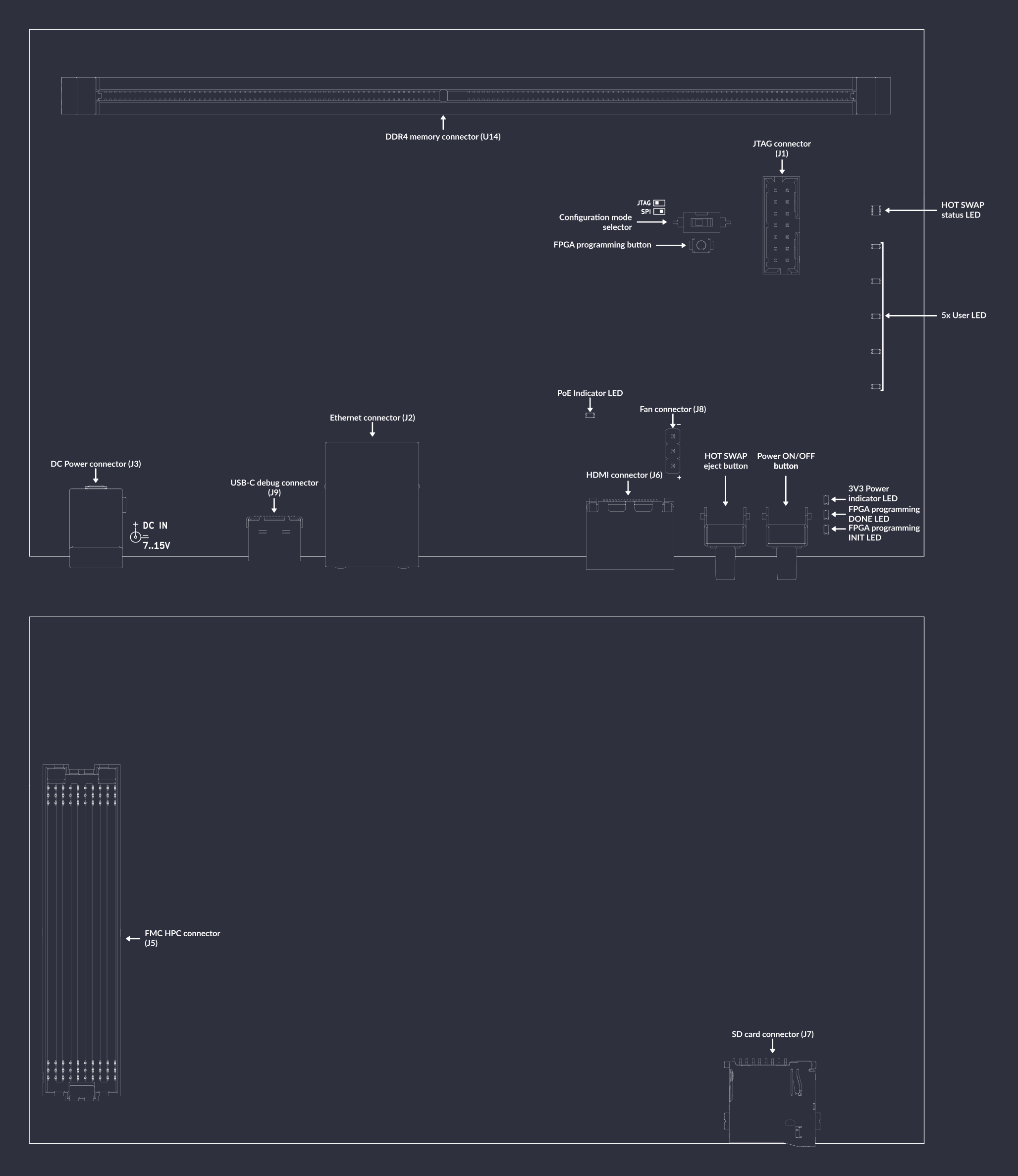
A map of on-board connectors, status LEDs, control buttons and I/O interfaces is provided in Fig. 9 below.

Fig. 9 DDR4 data center dram tester interface map
Connectors:
J3- main DC barrel jack power connector, voltage between 7-15V is supportedJ9- USB-C debug connector used for programming FPGA or Flash memoryJ1- standard 14-pin JTAG connector used for programming FPGA or Flash memoryJ6- HDMI connectorJ2- Ethernet connector used for data exchange with on-board FPGA and power supply via PoEU14- 288-pin RDIMM connector for connecting DDR4 memory modulesJ8- optional 5V fan connectorJ7- socket for SD cardJ5- FMC HPC connector reserved for future use
Switches and buttons:
Power ON/OFF button
S3- push button to power up the device, hold for 8s to turn off the deviceFPGA programming button
PROG_B1- push button to start programming from FlashConfiguration mode selector
S2- Switch left/right to specify SPI/JTAG programming modeHOT SWAP eject button
S1- reserved for future use to turn off DDR memory and allow hot swapping it
LEDs:
3V3 Power indicator
PWR1- indicates presence of stabilized 3.3V voltagePoE indicator
D15- indicates negotiated PoE voltage supplyFPGA programming INIT
D10- indicates current FPGA configuration stateFPGA programming DONE
D1- indicates completion of FPGA programmingHOT SWAP status
D17- RGY LED indicating status of hot swap process
Board configuration
Connect power supply (7-15VDC) to J3 barrel jack.
Then connect the board USB cable (J9) and Ethernet cable (J2) to your computer and insert the memory module to the socket U14.
To turn the board on, use power switch S3.
After power is up, configure the network and prepare the board for uploading the bitstream.
A JTAG/SPI switch S2 on the right side of the board (near the JTAG connector) defines whether the bitstream is loaded via JTAG or SPI Flash memory.
Bitstream will be loaded from flash memory upon device power-on or after pressing the PROG_B1 button.