RDIMM DDR5 Tester
The RDIMM DDR5 Tester is an open source hardware test platform that enables testing and experimenting with various DDR5 RDIMMs (Registered Dual In-Line Memory Module).
The hardware is open and can be found on GitHub.
For FPGA gateware documentation for this board, refer to the Gateware Documentation chapter.
Variants
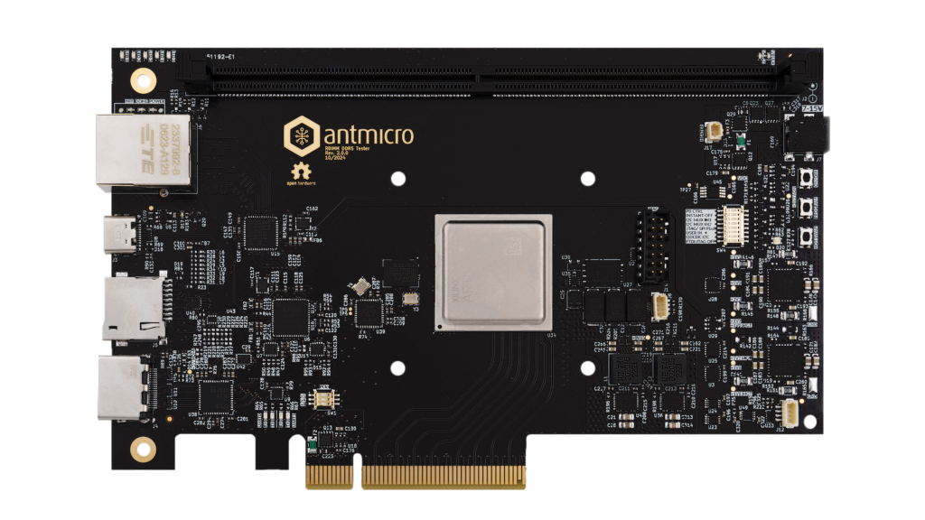
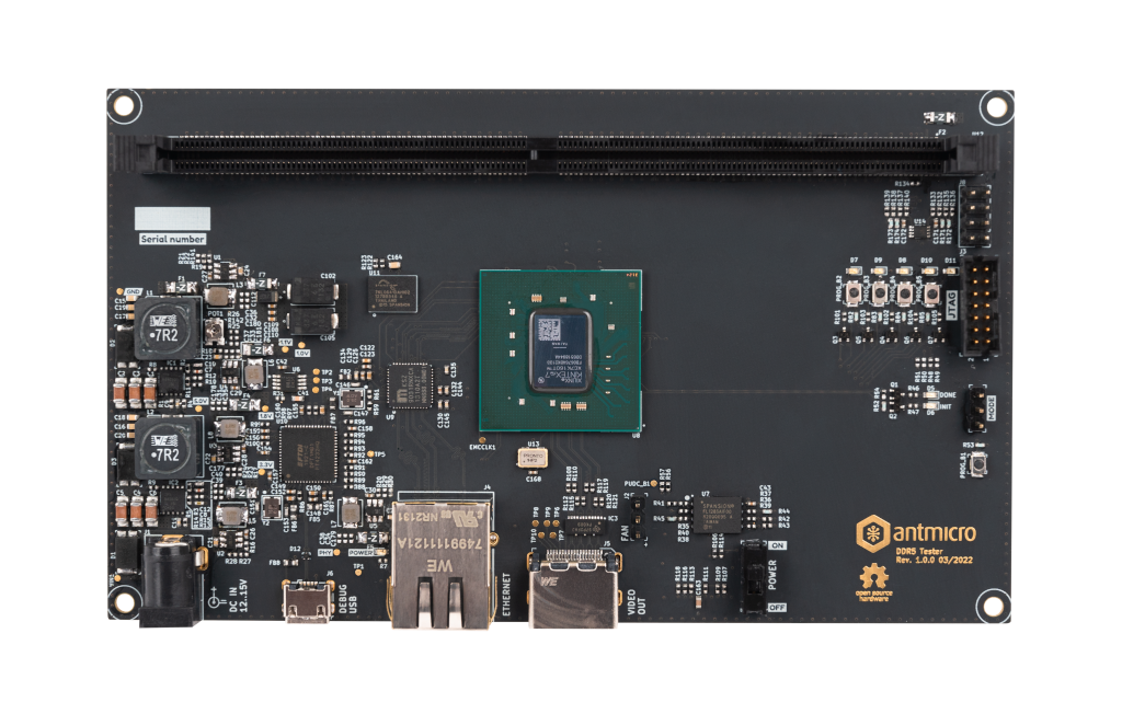
The latest design revision (Rev. 2.0) is based on AMD (Xilinx) UltraScale Plus FPGA which offers more logic resources operating at higher throughput. A more detailed comparison between Kintex-7 and UltraScale Plus RDIMM DDR5 Tester can be found in this blog note.
IO map
A map of on-board connectors, status LEDs, control buttons and I/O interfaces is provided in Fig. 6 below.
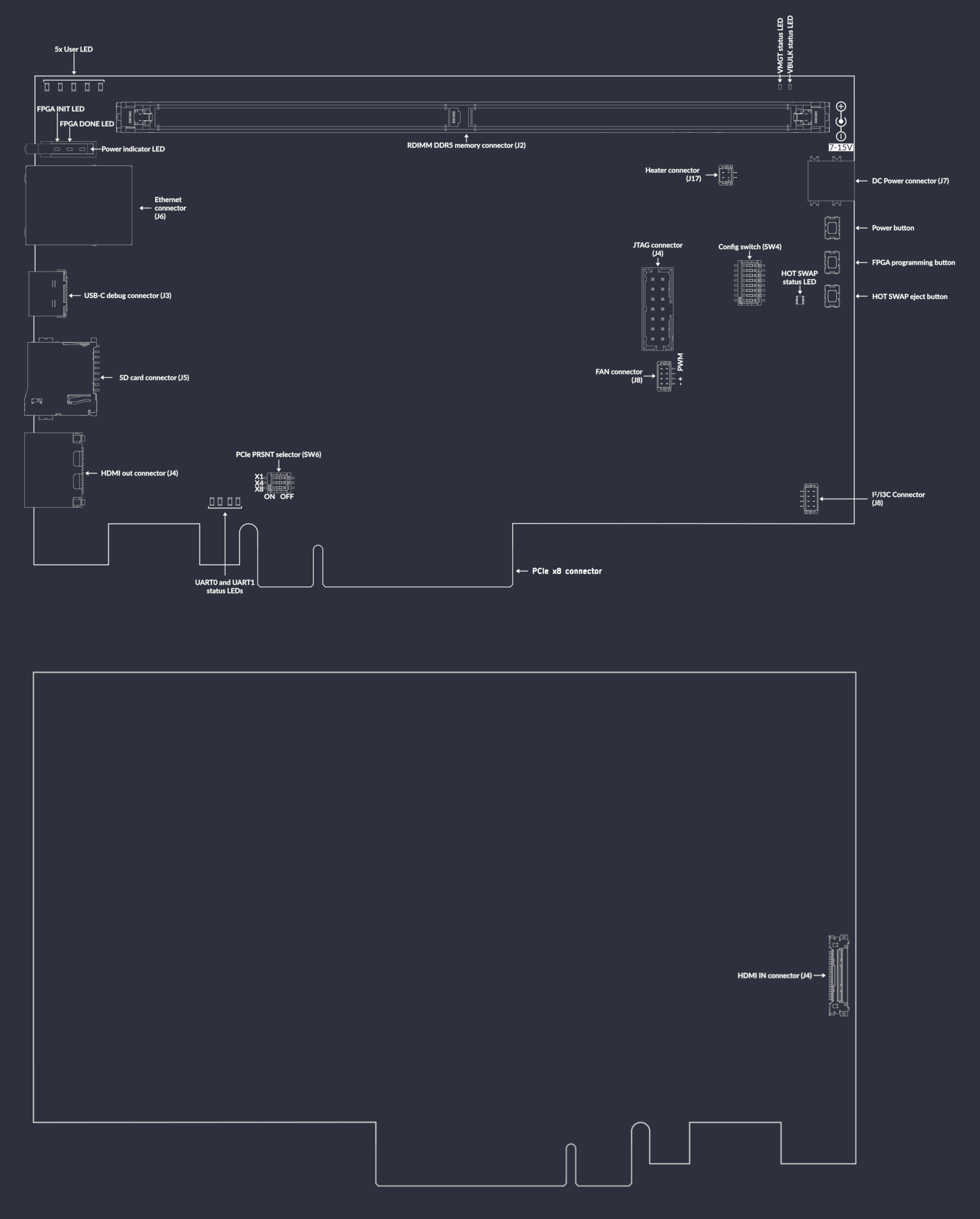
Fig. 6 DDR5 tester interface map
Connectors:
J7- main DC barrel jack power connector, voltage between 7-15 V is supportedJ3- USB-C debug connector used for programming FPGA or Flash memoryJ4- HDMI output connectorJ11- HDMI input connectorJ6- Ethernet connector used for data exchange with on-board FPGAJ2- 288-pin RDIMM connector for connecting DDR5 memory modulesJ8- optional 5V fan connectorJ5- socket for SD cardJ12- I2C/I3C connectorJ17- Heater connector (maximum 10W)J1- optionally mounted standard 14-pin JTAG connector used for programming FPGA or Flash memory
Switches and buttons:
Power button
SW5- push button to power up the device, push button again to turn the device offFPGA programming button
SW2- push button to start programming from FlashPCIe present selector
SW1- switch slide to set PCIe present to X1, X4 and X8HOT SWAP eject button
SW3- reserved for future use to turn off DDR memory and allow hot swapping itConfig switch
SW4- switch for setting several configuration options (options described later)
LEDs:
Power good indicator
D1- indicates presence of all FPGA voltage rails stabilizedFPGA programming INIT
D2- indicates current FPGA configuration stateFPGA programming DONE
D3- indicates completion of FPGA programmingVBULK indicator
D21- indicates presence of VBULK DDR5 voltage rail stabilizedVMGT indicator
D22- indicates presence of VMGT DDR5 voltage rail stabilized
A map of on-board connectors, status LEDs, control buttons and I/O interfaces is provided in Fig. 7.
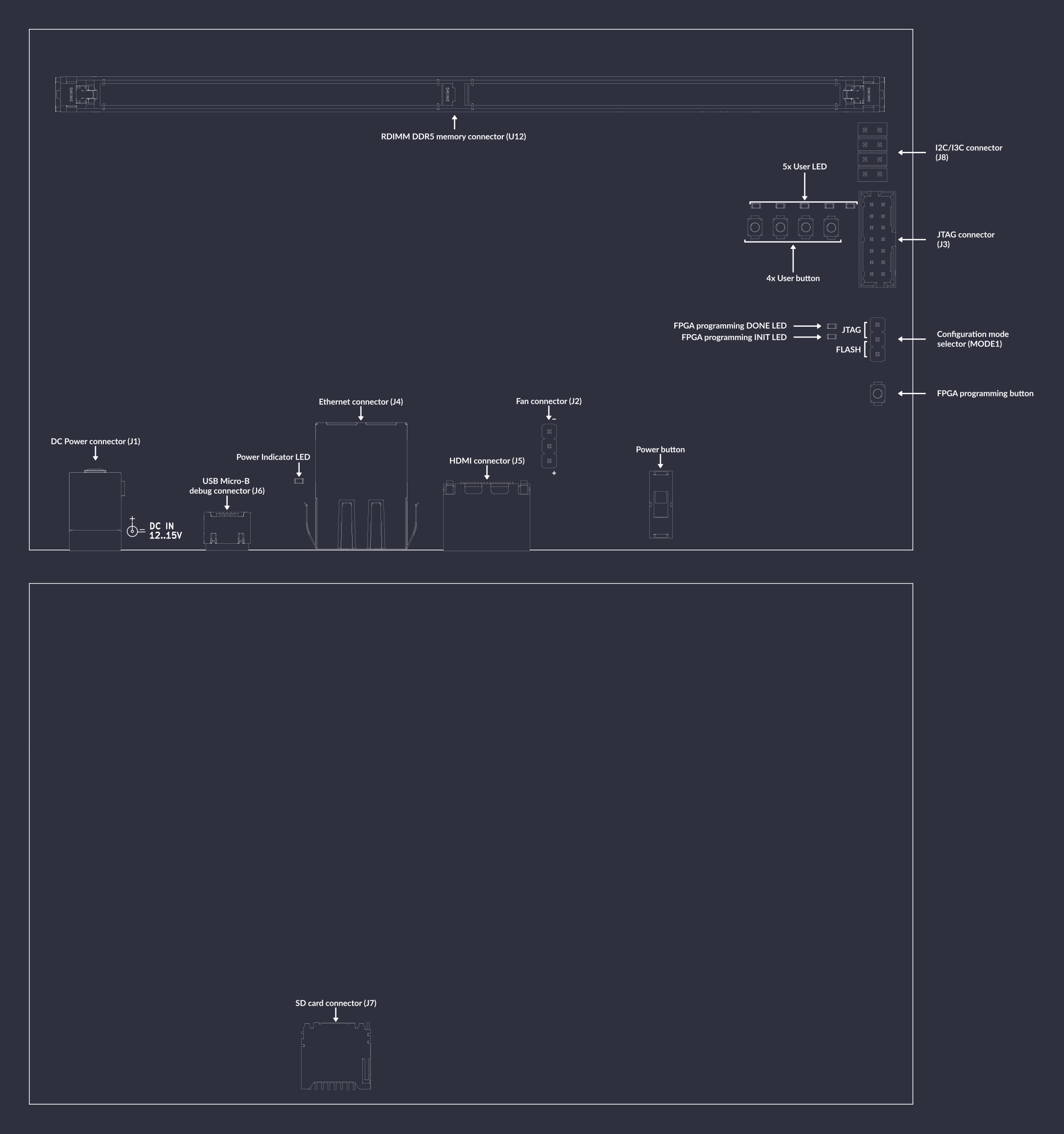
Fig. 7 DDR5 tester interface map
Connectors:
J1- main DC barrel jack power connector, voltage between 12-15V is supportedJ6- USB Micro-B debug connector used for programming FPGA or Flash memoryJ3- standard 14-pin JTAG connector used for programming FPGA or Flash memoryJ5- HDMI connectorJ4- Ethernet connector used for data exchange with on-board FPGAU12- 288-pin RDIMM connector for connecting DDR5 memory modulesMODE1- configuration mode selector, short proper pins with jumper to specify programming modeJ2- optional 5V fan connectorJ7- socket for SD cardJ8- 2.54mm goldpin connector with exposed I2C and I3C signals
Switches and buttons:
Power ON/OFF button
S1- slide up to power up a device, slide down to turn off the deviceFPGA programming button
PROG_B1- push button to start programming from Flash4x User button (
PROG_B2,PROG_B3,PROG_B4,PROG_B5) - user-configurable buttons
LEDs:
Rowhammer Tester Target Configuration
The following instructions explain how to set up the board depending on the revision you have.
Set the config switch SW4 in proper positions.
The possible options are:
PB- CTRL - automatically turn on board or use power button
SW5INSTANT OFF - pushing power button
SW5will turn off device instantly or after 8sI2C MUX IN1 - configure switch of I2C on board (described below)
I2C MUX IN2 - configure switch of I2C on board (described below)
JTAG/ SPI Flash - boot mode switch
USER IN - User configurable input
QDCDC2 I2C - enable I2C in main DCDC converter
FTDI JTAG OFF - disable on-board FTDI which communicates with FPGA and Flash memory via JTAG
Configure power-up of I2C on board:
PWR I2C |
IN1 |
IN2 |
|---|---|---|
OFF |
L |
L |
FPGA DDR I2C |
H |
L |
FPGA PWR I2C |
L |
H |
FTDI |
H |
H |
Connect power supply (12-15VDC) to the J1 barrel jack.
Then connect the board USB cable (J6) and Ethernet cable (J4) to your computer and insert the memory module to the socket U12.
To turn on the board, use the power switch S1.
After power is up, configure the network and upload the bitstream.
There is a JTAG/SPI switch (MODE1) on the right-hand side of the board.
Unless it’s set to the SPI setting, the FPGA will load the bitstream received via JTAG (J3).
The bitstream will be loaded from flash memory upon device power-on or after pressing the PROG_B1 button.
Simulation
The simulation is based on a DDR5 DRAM model (sdram_simulation_model.py) and a DDR5 PHY simulation model (simphy.py). These models are used by the SoC simulation model (simsoc.py).
Start the simulation with:
python3 third_party/litedram/litedram/phy/ddr5/simsoc.py --no-masked-write --with-sub-channels --dq-dqs-ratio 4 --modules-in-rank 1 --log-level error --skip-csca --skip-reset-seq --skip-mrs-seq --with-prompt --l2-size 256 --uart-name serial