SO-DIMM DDR5 Tester

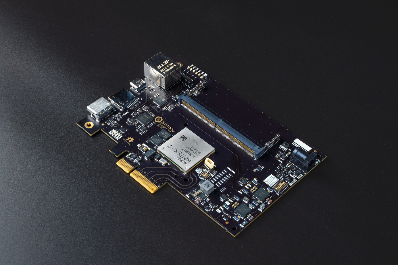
Fig. 2 SO-DIMM DDR5 Tester
The SO-DIMM DDR5 tester is an open source hardware test platform that enables testing and experimenting with various off-the-shelf DDR5 SO-DIMM modules. This board also supports testing single LPDDR5 ICs via LPDDR5 Test Bed.
The hardware is open and can be found on GitHub: https://github.com/antmicro/sodimm-ddr5-tester
For FPGA digital design documentation for this board, refer to the Digital design chapter.
IO map
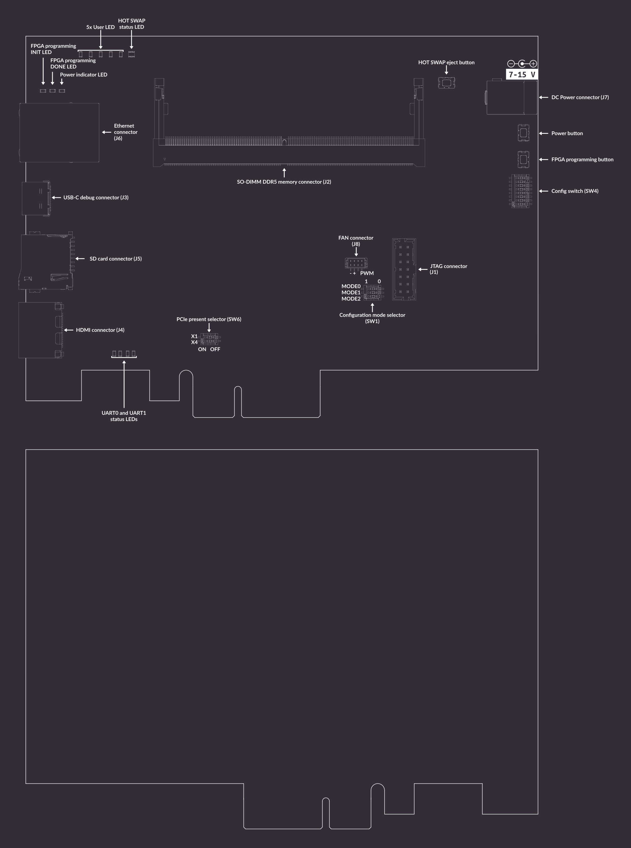
A map of on-board connectors, status LEDs, control buttons and I/O interfaces is provided in Fig. 3 below.

Fig. 3 SO-DIMM DDR5 tester interface map
Connectors:
J7- main DC barrel jack power connector, voltage between 7-15 V is supportedJ3- USB-C debug connector used for programming FPGA or Flash memoryJ1- optional slot for a standard 14-pin JTAG connector used for programming FPGA or Flash memoryJ4- HDMI connectorJ6- Ethernet connector used for data exchange with on-board FPGAJ2- 262-pin SO-DIMM connector for connecting DDR5 memory modulesJ8- optional 5V fan connectorJ5- socket for SD card
Switches and buttons:
Power button
SW5- push button to power up the device, push button again to turn the device offConfiguration mode selector
SW1- switch proper slides to specify programming mode (options described later)FPGA programming button
SW2- push button to start programming from FlashPCIe present selector
SW6- switch slide to set PCIe present to X1 and X4HOT SWAP eject button
SW3- reserved for future use to turn off DDR memory and allow hot swapping itConfig switch
SW4- switch for setting several configuration options (options described later)
LEDs:
3V3 Power indicator
D1- indicates presence of stabilized 3.3V voltageFPGA programming INIT
D3- indicates current FPGA configuration stateFPGA programming DONE
D2- indicates completion of FPGA programmingHOT SWAP status
D9- RGY LED indicating status of hot swap processUART0 and UART1 status (
D10,D11,D12,D13) - indicates status of RX/TX lines of UART protocols
Rowhammer Tester Target Configuration
The following instructions explain how to set up the board.
Set configuration mode selectors SW1 in proper positions.
Using these 3 switches, you can set the following modes:
Configuration mode |
MODE[2] |
MODE[1] |
MODE[0] |
|---|---|---|---|
Master Serial |
0 |
0 |
0 |
Master SPI |
0 |
0 |
1 |
Master BPI |
0 |
1 |
0 |
Master SelectMAP |
1 |
0 |
0 |
JTAG |
1 |
0 |
1 |
Slave SelectMAP |
1 |
1 |
0 |
Slave Serial |
1 |
1 |
1 |
For JTAG programming, set JTAG mode.
If the bitstream needs to be loaded from the Flash memory, select Master SPI mode.
This configuration is set by default.
The bitstream will be loaded from flash memory upon device power-on or after a SW2 button press.
Set config switch SW4 in proper positions.
The possible options are:
PB- CTRL - automatically turn on board or use power button
SW5INSTANT OFF - pushing power button
SW5will turn off device instantly or after 8sI2C MUX IN1 - configure switch of I2C on board (described below)
I2C MUX IN2 - configure switch of I2C on board (described below)
PWR I2C SDA - disable I2C in 3V3 powered IC’s
PWR I2C SCL - disable I2C in 3V3 powered IC’s
QDCDC2 I2C - enable I2C in main DCDC converter
FTDI JTAG OFF - disable on-board FTDI which communicates with FPGA and Flash memory via JTAG
Configure power-up of I2C on board:
PWR I2C |
IN1 |
IN2 |
|---|---|---|
OFF |
L |
L |
FPGA DDR I2C |
H |
L |
FPGA PWR I2C |
L |
H |
FTDI |
H |
H |
Connect power supply (7-15VDC) to J7 barrel jack.
Then connect the board’s USB-C J3 and Ethernet J6 interfaces to your computer, insert the memory module into the J2 socket and turn it on using power switch SW5.